Opinion
Can China repeat its electric vehicle leapfrog with semiconductors?
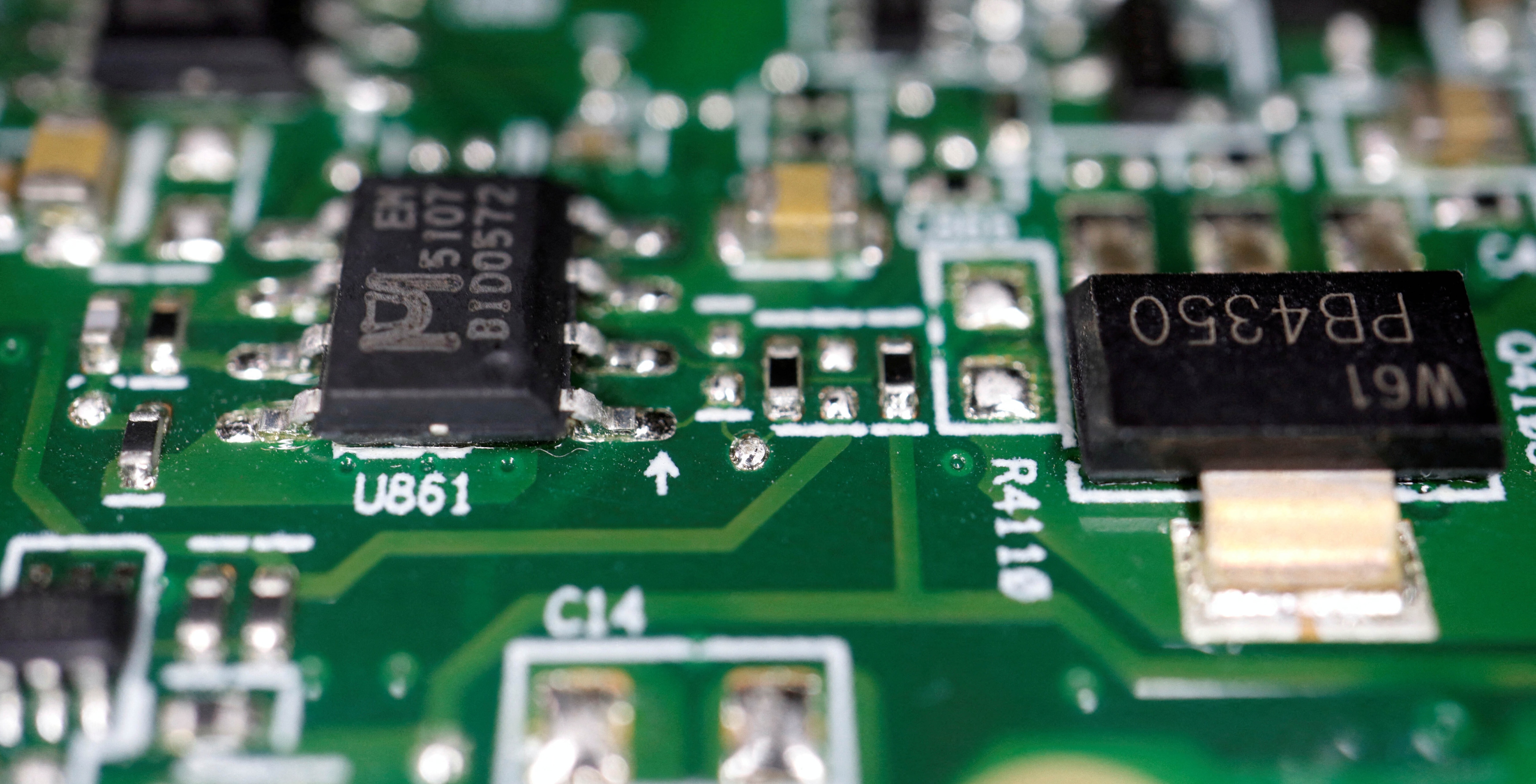
China lacks access to extreme UV lithography technology needed to build advanced chips. Image: REUTERS/Florence Lo
- AI was top of the agenda at the recent US-China summit, as the two countries race for dominance in an industry reliant on semiconductors.
- China lacks access to extreme UV lithography technology needed to build advanced chips and scale up its AI industry, due to US export controls.
- Instead, China is looking to replicate its success in the EV sector by leapfrogging to next-generation semiconductor architectures beyond better lithography, to build the most powerful AI chips required for the future.
Artificial intelligence (AI) was top of the agenda when Xi Jinping arrived in Washington, DC to meet with Donald Trump last month. "Whoever wins AI, wins," the US President proclaimed ahead of what was the second summit between the two leaders.
How close is this race? The White House's own AI adviser says the US lead is as little as six to nine months. In terms of human history, that is a photo finish.
But the two sides are short of different resources. While the US has the chips but is running out of electricity, China has power but is short of advanced chips. Remedying the semiconductor gap is China’s #1 technology priority.
The machine China cannot buy
China’s most glaring shortage is one of the most complicated objects mankind has ever built – extreme ultraviolet (EUV) lithography – developed and sold only by the Netherlands’ ASML.
The newest version costs roughly $400 million. EUV is how every advanced chipmaker on Earth prints features below the 7-nm node, to pack transistors tight and get more computing per square millimeter of semiconductor material. And the US has locked China out of buying it.
China has tried to build its own EUV technology, but it has gone slowly. This past summer it was reported that China had begun small-batch production of its first home-grown immersion deep-ultraviolet (DUV) scanner. It is roughly four generations behind, or so far behind the frontier that the equivalent machine, ASML’s TWINSCAN NXT:1950i launched in 2008, is not even on the export control list.
How are Chinese engineers and scientists innovating around constraints?
How China overtook others on EV innovation
There’s a strategic phrase in China – 弯道超车, meaning "overtaking on the bend” – because it is much harder to pass a vehicle when the road is straight. China famously ran this playbook with automobiles.
They realized that if they devoted 100% of their effort to catching up on internal-combustion engines, success would mean they’d still only be one of the roughly 20 gargantuan global auto firms competing among the likes of Ford, Toyota and Volkswagen.
Instead, China bet on then-nascent electric vehicles (EVs) as the next platform – a technology leapfrog. The bet was formalized in their “863 Electric Vehicle Programme” starting in their 10th Five-Year Plan (2001-2005), followed by the 2009 "Ten Cities, Thousand Vehicles" initiative.
The ambition paid off. Chinese automakers supplied 60% of global EV sales by 2025, and China has passed Germany and Japan to become the world's largest vehicle exporter.
Applying the same principles in silicon
Chinese chipmakers do not only want to close the gap on existing silicon; they want to lead.
The clearest example is the Tau (τ) Scaling Law, revealed this past summer as a potential successor to Moore's Law – the storied prediction that computing power will increase significantly as the number of transistors on microchips doubles about every two years (with cost per transistor falling along the way). This is the culmination of Huawei investing 22 years in chip R&D to establish their independence.
Tau is the Greek letter for t, shorthand for a time constant. The idea here is to stop optimizing transistor size, which is what EUV buys you, and optimize for the time a signal takes to cross between transistors, between chips, and between servers.
Its essence is that shorter wiring, lower electrical resistance and capacitance, and better coordination across chips will enable computations to finish faster and use less energy without relying solely on smaller transistors.
For example, in a large AI cluster, more than 80% of the energy goes to moving data through wires, rather than computing in the transistor gates. So, it is a potential game-changer to shorten the wires between transistors that frequently talk to each other.
One way to achieve this is to go three-dimensional. One of Huawei’s techniques, LogicFolding, splits the busiest blocks of a chip across two vertically bonded tiers, turning long horizontal runs into short vertical hops.
This is not just 3D stacking, as Huawei is going much further than anyone else – they are designing logic across the two tiers as one circuit from the outset. Think of conventional chip stacking as two office towers designed independently, and then connected by walkways at their front doors. Huawei’s LogicFolding, meanwhile, designs one building from the start, with stairwells and plumbing laid out across floors as a single system.
This results in far denser vertical connections – roughly 10-40 times more per unit area than the best TSMC or Intel run in high-volume production today. And this is no lab experiment: the first chip built this way went on sale this September, inside Huawei's Mate XT2 trifold phone.
Admittedly, the technique is easier to pull off on a small phone chip than on a large AI processor. But on that phone chip, transistor density rose 55% and power consumption fell 41% on its CPU, with similar boosts on its GPU and NPU.
Chinese memory companies went radically 3D, too. YMTC commercialized wafer-to-wafer hybrid bonding in 2019 under its Xtacking architecture, and built a substantial patent position around it.
In 2025, Samsung reportedly licensed YMTC’s hybrid-bonding intellectual property as it moved towards 400+ layer bonded NAND. Meanwhile Kioxia and SK Hynix are pursuing similar architectures. A Chinese semiconductor tech path is rapidly becoming an industry standard.
Light is another lane of innovation. Photons carry data far more cheaply than electrons over distance, and here Huawei is investing heavily; for example, it introduced a 7.2 terabit-per-second near-packaged optics module, a shade ahead of Broadcom. And Huawei SuperPoD systems have wired 8,192 accelerators into a single system over optical fibre, whereas Nvidia still runs more copper inside the rack.
Chinese companies are now at the frontier in making truly 3D chips, at replacing electrons with light, and at optimizing the whole data centre.
Moore's Law was never just about small transistors
Here is the part that makes this everyone’s concern: Moore's Law has been dying for a decade.
Smaller and denser is how Moore’s Law gets framed, though the whole point was supposed to be that shrinking made transistors cheaper – that is, more performance per dollar. But that bargain has broken. One telltale sign is that when ASML shipped its newest EUV machine, TSMC initially declined to buy, saying it was too pricey to use.
Every chipmaker worldwide will need techniques beyond better lithography. That means looking to novel architectures like 3D and photonics to keep the cost-performance curve falling. And China started chasing these approaches early, because they had to innovate.
All signs point to chipmakers outside of China increasingly wanting to license semiconductor techniques developed inside of China, as Samsung already has with YMTC's bonding patents.
How China can drive semiconductor innovation
Nevertheless, lack of access to EUV remains a major handicap.
Given China’s manufacturing prowess, it may be surprising to learn that Epoch AI estimates Huawei will produce less than 4% of Nvidia's AI compute in 2026, and Huawei’s chips will continue to trail Nvidia’s in per-chip performance by three to four years until at least 2030.
Huawei's own target for frontier-equivalent transistor density is 2031. Even that would be matching what TSMC ships at scale today, and TSMC will not stand still.
Can China repeat the electric vehicle leapfrog in chips? The moat that must be crossed in semiconductors is deeper. But China does not need to win outright in order to change the road everyone else drives on.
Set the geopolitics aside for a moment.
Chinese engineers’ and companies’ willingness to walk an untested R&D path is a big addition to the innovative capacity of mankind. One unintended consequence of export controls is that they have split one semiconductor roadmap into two, and two independent pursuits can cover more of the design space than one ever did. And, many of the techniques Chinese engineers have pioneered can be used in combination with EUV lithography.
It may well be that the most powerful AI chips in the future will carry fingerprints from both East and West.
Don't miss any update on this topic
Create a free account and access your personalized content collection with our latest publications and analyses.
License and Republishing
World Economic Forum articles may be republished in accordance with the Creative Commons Attribution-NonCommercial-NoDerivatives 4.0 International Public License, and in accordance with our Terms of Use.
The views expressed in this article are those of the author alone and not the World Economic Forum.

Forum Stories newsletter
Bringing you weekly curated insights and analysis on the global issues that matter.
More on Artificial IntelligenceSee all

E. Richard Gold
September 30, 2026


