The next climate breakthrough may come from materials too small to see

Materials innovation needs to move beyond slow trial-and-error Image: REUTERS/Herwig Prammer
- Common bottlenecks to durable clean technologies and other global challenges happen at invisible interfaces between materials.
- An interface material can help extend product lifetime, reduce failure rates and improve manufacturing yield.
- Materials innovation needs to move beyond slow trial-and-error through artificial intelligence connected to physical experimentation and an integrated learning system to achieve more autonomous outcomes.
When people imagine the technologies that will shape the next industrial era, they often picture things that are wholly visible: solar farms, electric vehicles, wind turbines, semiconductor fabs, satellites, robots or medical devices.
Yet many of the breakthroughs that determine whether these technologies succeed occur at scales almost invisible to the human eye.
They happen at interfaces: where one material meets another.
A solar cell loses efficiency because a thin layer degrades. A copper interconnect in advanced chip packaging fails because it does not adhere well enough to the glass substrate. A sensor in the human body corrodes because its protective coating is imperfect.
These may sound like niche engineering problems. They are not. They are bottlenecks in the global transition to cleaner energy, more resilient supply chains, better healthcare and more advanced technologies.
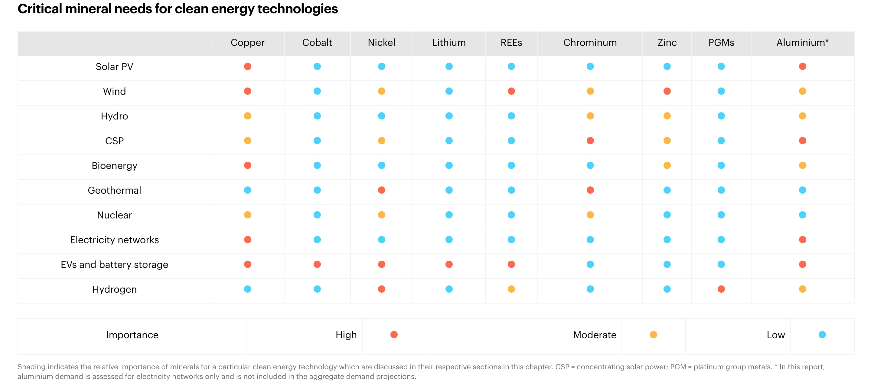
The world is already discovering that the energy transition is also a materials transition. The International Energy Agency has shown that clean energy technologies, from solar panels and wind turbines to electric vehicles and battery storage, require a wide range of minerals and metals.
The challenge has been to produce more clean technologies but we must also make them more durable, efficient and resource-conscious.
The solution cannot simply lie in extraction. We need more responsible mining, recycling and circular supply chains but humanity also needs better materials that can do more with less.
How interface materials can enhance clean technologies
That is where interface materials come in.
An interface material is often extremely thin but its impact can be large. It can help two surfaces bond, protect a sensitive component from oxygen, water, heat or corrosion and guide the movement of electrons inside a device and support charge transport.
It can extend product lifetime, reduce failure rates and improve manufacturing yield. A small material layer can determine whether a large technology becomes practical, affordable and durable.
Some of these materials already have names familiar to scientists, though not yet to the public. Self-assembled monolayers, often called SAMs, are molecular layers that organize on surfaces and can tune how other materials grow, transport charge or resist degradation.
Silane coupling agents can help connect glass, oxides, polymers and metals, improving adhesion in electronics, coatings and packaging. Ultra-thin encapsulation or barrier materials can protect sensitive devices from water, oxygen, ions or biological fluids.
These materials may be measured in nanometers but their consequences can be measured in years of product life, percentage points of efficiency, tons of avoided waste and billions of dollars of manufacturing value.
The lesson is that the smaller the material, the more important it is to understand the system around it.
A promising molecule is not enough. It must work on a real substrate, survive a real manufacturing process, remain cost-effective, safe, and scalable and perform reliably over time. That complexity is why materials innovation needs to move beyond slow trial and error.
Why better and integrated information is critical to materials innovation
Artificial intelligence (AI) can help compress this timeline but only if it is connected to physical experimentation. In materials science, data is often fragmented, incomplete or inconsistent.
A model trained on poor experimental data will not produce reliable answers on its own. The real opportunity is to build closed-loop systems: AI proposes candidates, automated or high-throughput experiments test them, results are fed back into the model and scientists guide the next round.
This approach is sometimes described as a “self-driving lab.” Research published in Nature has shown how autonomous laboratories can combine computation, literature-derived data, machine learning, active learning and robotics to accelerate materials synthesis.
These systems point to a future in which experiments are not isolated events but part of a continuous learning loop. Yet, the true bottleneck is not only the AI model. It is the quality of the knowledge flowing into it.
Many laboratories still record experiments as disconnected spreadsheets, notebook entries, images and instrument files. However, for AI, a result is useful only if it is context-dependent.
What was the substrate? How was it cleaned? What was the humidity? Which precursor batch was used? What were the coating conditions, drying time, equipment status and environmental variables?
Without structured data, two experiments that look identical on paper may be completely different in reality.
How we can accelerate interface materials innovation
This is why high-throughput experimentation should not simply mean doing more experiments faster. It should mean designing experiments so each one produces reusable knowledge. The future materials laboratory must integrate molecules, equipment, process data, and performance results into a single learning system.
This closed-loop learning system is evident in Pheno’s AI-assisted materials discovery platform, where high-throughput experimentation, AI-assisted molecular design and structured experimental data are combined into a continuous feedback loop.
Candidate molecules can be proposed, synthesized or selected, tested across relevant substrates and process conditions, and then evaluated through performance and reliability data.
Each result helps improve the next round of design, allowing interface materials to be discovered and optimized far more quickly than through traditional trial-and-error methods.
By connecting design, experimentation and feedback into one learning cycle, this system can shorten materials discovery from what once required years of research to just a few months.

Why shorter discovery time can help solve global challenges
For global challenges, this matters in three ways.
Faster materials discovery can reduce pressure on scarce resources. If a new interface layer improves device lifetime or manufacturing yield, fewer materials may be wasted.
Better materials can make clean technologies more bankable. Investors, utilities and customers do not buy laboratory records; they buy reliable performance over years.
AI-enabled materials platforms can broaden participation in innovation. More standardized data, modular automation and shared testing methods could allow more regions and industries to solve local problems with advanced tools.
The next phase of climate and industrial innovation will not be won only by building bigger factories or extracting more minerals. It will also be won by understanding the invisible layers that make technologies last.
A molecule that helps copper adhere to glass may support the next generation of chip packaging. A protective coating may extend the life of a sensor. A self-assembled monolayer may improve the performance of a solar cell.
None of these examples alone solves climate change, resource scarcity or technological inequality. Together, however, they point to a larger truth: small materials can unlock large systems.
If the world wants cleaner energy, more resilient manufacturing and more inclusive technological progress, we must treat materials discovery as core infrastructure for the future.
The breakthroughs may be too small to see but their impact will be wholly in view.
Don't miss any update on this topic
Create a free account and access your personalized content collection with our latest publications and analyses.
License and Republishing
World Economic Forum articles may be republished in accordance with the Creative Commons Attribution-NonCommercial-NoDerivatives 4.0 International Public License, and in accordance with our Terms of Use.
The views expressed in this article are those of the author alone and not the World Economic Forum.
Stay up to date:
Advanced Materials

Forum Stories newsletter
Bringing you weekly curated insights and analysis on the global issues that matter.
More on Technological InnovationSee all

Kary Bheemaiah and Ann Cleaveland
July 22, 2026


